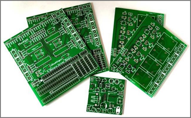
PCB boards are all around us in every gadget we use. Be it the smartphone or a simple calculator, their function depends on the performance of PCBs.
Do you know what the PCB circuit boards made of are? PCB vs. PCBA-What are the differences? Have you ever opened up your iPhone to see what’s inside? You would find only a few things, from the digitizer, battery to soldering, and of course, the PCB.
The logic board is what keeps your iPhone running, and any damage to it results in your phone not being able to power on again. The compact circuit board design of the iPhone X, for instance, has wowed many analysts and techies. It is a feat of engineering that not many companies have been able to surpass.
So, what is it that makes circuit boards so unique? What makes one circuit board better than the other? What does a circuit board consist of?
We have prepared this helpful guide where you can learn about the materials used to make PCBs. You can also get a picture of how a manufacturer produces them. Let’s begin by taking a look at what are the circuit boards made of. Then, we will take a look at how you can make your circuit boards.
- What is the PCB Circuit Boards Made Of: This section gives a brief overview of the PCB board composition.
- What material is the board made of: This section details the PCB usually made of four layers of material, made of the substrate, copper, solder mask, and wire mesh. And are also introduced to their respective characteristics.
3. Custom Board: This section focuses on two significant steps of the custom board: Prepare Schematic View, Access Board Layout View.
4. How are Circuit Boards Made: By now, you know how to custom design your PCB by reading the earlier chapter. The technology of PCB is complicated, and it needs to go through a multi-stage manufacturing process. You also have to choose a manufacturer who has all the high precision equipment to bring your project to life. We are going to discuss the PCB manufacturing process in brief just for you.
1. Making the Substrate
You can think of PCBs as sandwiches that come in multiple layers. The base material that is found in the middle is known as the substrate. Then the substrate material is responsible for giving width to the PCB. You can view a PCB from the side angle and find that the thickest layer is the substrate.
Traditionally PCBs were made with fiberglass substrate, which is rigid. Nowadays, you can find a flexible substrate material. Many articles can be, but one standard option is using special plastic for the substrate, which can tolerate high temperatures.
The material used to make the substrate is generally spread out, the manufacturer then dips it or sprays it with epoxy resin. Next, the material is rolled on to get the desired thickness just like you roll your pie crust using a rolling pin.
The rollers stop rolling when the substrate reaches the desired thickness and passes to the next step, and the substrate is now placed in the oven so that it turns out solid and firm by curing it. After the completion of this step, you have created the very first layer of your PCB.
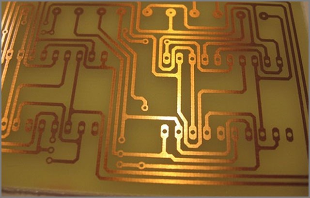
2. The Copper Layers
The copper layers are essential to carry electricity throughout your PCB. Depending on the purpose, PCBs have a simple or complex design. Apart from the foundation layer of the substrate, copper layers are another essential component.
Your PCB cam comes with a single layer of copper applied to the top or two layers on both sides of the substrate. The PCB can also have numerous layers with other copper and substrate. Some PCBs used in advanced devices or smartphones have more than 12 or 16 layers of copper.
Copper layers are much lesser in width than the substrate layers, and you won’t have any electricity flowing through your circuit if they are absent.
The manufacturer can use a combination of different methods to bond the copper to the surface of the substrate. Any standard methods involve using heat, pressure, and adhesive so that the copper layers are fixed firmly on the substrate. You can take your PCB for drilling after the copper has bonded with the substrate.
For your device to function, the PCB needs to transmit the charge to the right points from one layer to another layer in the board. You will have to create holes referred to as via for the cost to be able to flow through. The manufacturer has several options to drill holes on the PCB and may use a CO2 laser, UV laser, or other equipment.
The accuracy and efficiency of the drilling machine determine the preciseness and complexity of the PCB.
You have to clean the holes of any debris or any material that might have been left behind after the process of drilling. They can also be deburred to get any additional material clinging to the PCB. After that, the inner sides of the vias are coated with copper so that it can carry the charge from one layer of the circuit board to another.
Next, you have to print the pattern of the circuit on the PCB. The manufacturer can deploy the copper accurately following the design to get the pattern on board. Otherwise, they may apply copper to the entire board and then remove the copper to etch out the circuit pattern.
The PCB may be subjected to an alkaline bath to remove any extra unnecessary copper.
What you need to add now is the other components such as transistors, capacitors, or LEDs on the PCB. You can solder the components on to the PCB using a soldering iron. Before adding the components, the PCB is passed through a succession of electrical tests using a grid tester or flying probe to ensure there are no short circuits or open connection.
Your manufacturer may also use a machine to pump out the parts to your PCB.
3. The Final Solder Mask
The metals which remain exposed on the circuit board have a chance to get damaged. The nature of copper is to destroy, which will render your PCB useless. You can adequately protect the copper plating and other components of the PCB by adding an extra protective layer on top.
Generally, manufacturers use gold, nickel, or tin-lead to plate specific vulnerable parts of the PCB. To top it all, the manufacturer provides another layer on top called the solder mask.
The green color that you see in PCBs is due to the application of the solder mask layer; the solder mask also has some other functions apart from covering and protecting all the metal parts that don’t need to form a connection with anything, the layer of solder mask also ensures that current flows to the right places following absolute paths.
Sometimes you may also find a layer of silkscreen on top of the solder mask, which is used to carve labels on necessary parts.
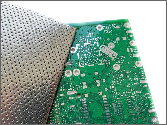
After everything is done, the manufacturer will trim and shed off any extra material or unnecessary parts that are not required in your PCB.
Circuit boards can be difficult to create, especially since there are many factors involved. For one, you need to ensure that you use copper and use the right soldering. Knowing what circuit boards are made of could help you see the circuit board you need for your business.
Creating circuit boards require adept knowledge and precision equipment. You also need to have a reliable and experienced manufacturer who can build PCBs accurately following your specifications. OurPCB can custom manufacturing of circuit boards to bring your project to life!